Photoresist Chemicals
Photoresist Chemicals for Advanced Semiconductor Photolithography
For over a decade, Halocarbon scientists and engineers have been partnering with leading suppliers to the semiconductor fabrication industry, development specialty fluorochemicals for use in next-generation semiconductor designs.
Halocarbon Science leverages a legacy of knowledge and expertise in organofluorine chemistry to develop unique solutions that help our partners drive advances in the electronics industry by enabling semiconductor miniaturization and enhancing semiconductor design.
| 193 Immersion Lithography | EUV & High tG Systems |
|---|---|
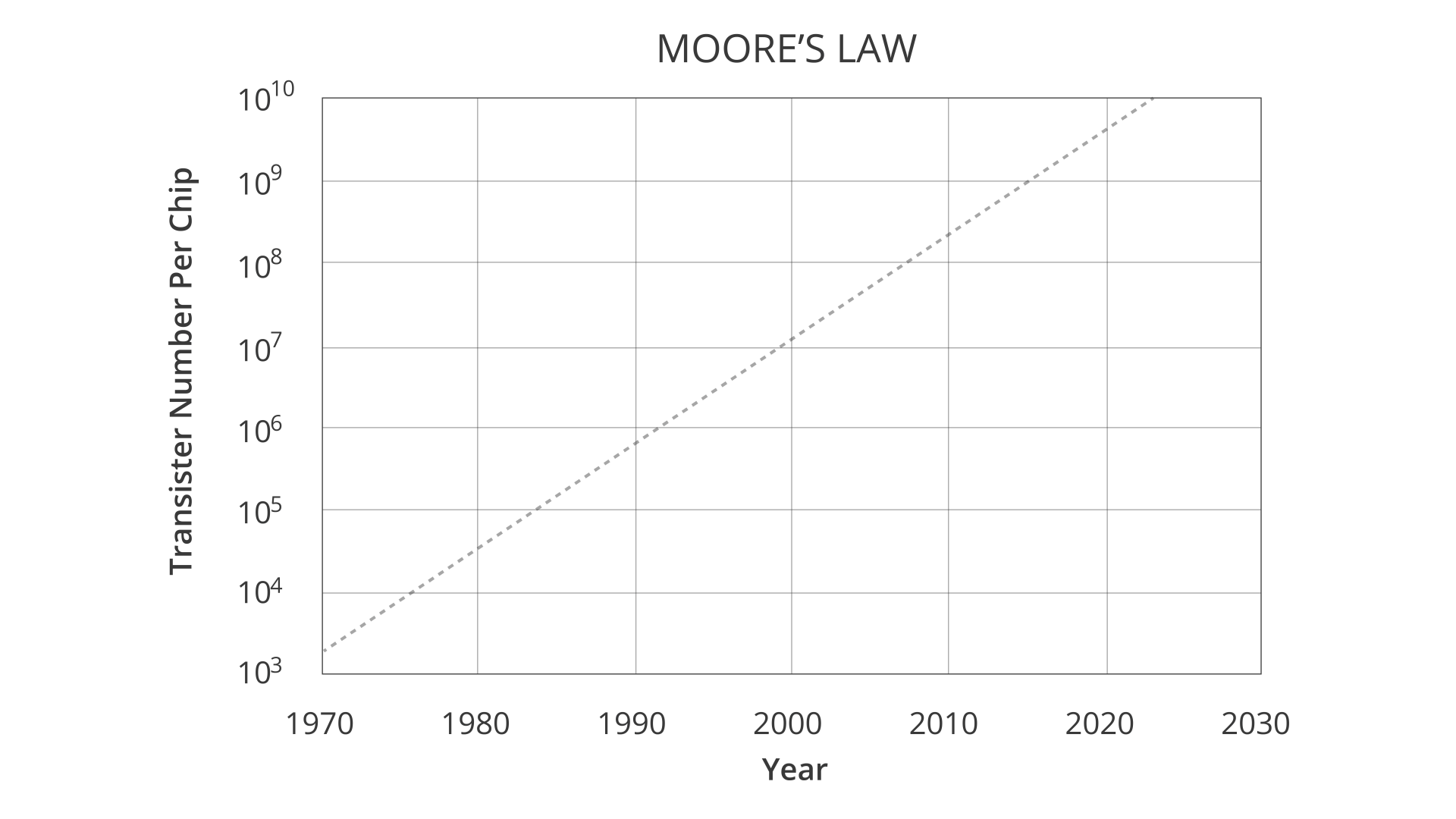
Keeping pace with Moore’s Law
In 1965, Gordon Moore, one of the co-founders of Intel, predicted that the number of transistors per integrated circuit would double every year.
After 50+ years, Moore’s seminal observation has been shown to still be true, serving as a map that sets the direction for the modern digital revolution. Implicit in Moore’s law is the demand for ancillary technologies to keep pace with ever-increasing circuit density.
These technologies include the methods and raw materials required to produce microprocessors with increasingly infinitesimal feature sizes.
EUV Lithography
Over the decades, semiconductors have been manufactured using photolithography. These processes involve the use of lasers of ever-decreasing wavelengths of light to etch circuits. Most modern processes use a broad range of radiation-sensitive polymeric films, reactive gases, and other chemicals in combination with physical equipment to create semiconductor highly-miniaturized microprocessors.
Extreme Ultraviolet (EUV) lithography is the most advanced lithographic process currently in use. This technology is being used on the most cutting-edge nodes – typically those at 5 nm or smaller in feature sizes.
While this technology has been in use for a few years, advances in EUV photoresists are required for its broad adoption. This is where Halocarbon fluorinated photoresist chemicals can be used to enhance the durability of EUV photoresists, providing high resistance to reactive ion etching (REI), especially when used as top anti-reflective coatings (TARCs)
Fluorochemistry in EUV Photolithography
EUV photoresists require high-Z elements like Tin, Hafnium, or Zirconium due to their optical density at EUV wavelengths. Fluorinated materials, however, can support and enhance these high-Z metal-based resists.
Fluorochemistry allows for:
- Plasma etch resistance – making them attractive as top anti-reflective coatings (TARCs)
- Low surface energy – allowing for resist adhesion control and lift-off processes
- Chemical resistance – minimizing outgassing while providing selective solubility parameters

193 Immersion Lithography
193 immersion lithography (193i) remains the most deployed photolithography technology in advanced semiconductor chip fabrication. This technology, when used in self-aligned double patterning (SADP) or self-aligned quadruple patterning (SAQP), can be used to achieve feature sizes down to 5 nm in size. These advanced processes require extreme control over the application, patterning, and development stages. Halocarbon has developed a portfolio of 193i monomer systems designed to provide manufacturers with the flexibility and control they seek in the design of new 193i photoresists.
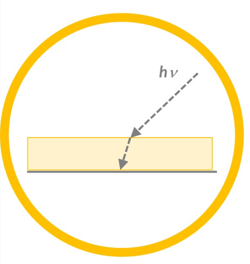
This figure describes the photolithography process at a high level, depicting the use of photoresist materials (photo-responsive polymeric coatings), photomasks (a patterning plate), and incident light to create circuit patterns ultimately used in a microprocessor design. In traditional photolithography, imaging is performed under an inert gas atmosphere, whereas immersion photolithography utilizes a water layer in contact with the substrate as a final lens element.
Hexafluoroisopropyl Chemistry
For over a decade, Halocarbon scientists and engineers have been partnering with leading manufacturers of the raw materials used in advanced photolithography processes. Halocarbon offers a broad range of high-purity electronics-grade monomers, monomer pre-cursors, and other specialty fluorochemicals for use in this process. Our key technologies leverage our expertise in producing hexafluoroisopropyl (HFIP) derivatives, which have been demonstrated to provide unique value to the semiconductor fabrication industry.
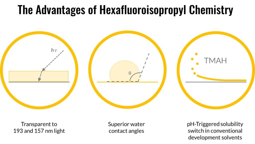
Transparency Control
In order to keep pace with Moore’s Law and to achieve better resolutions in photolithography, the chip manufacturing industry has employed light sources of progressively shorter wavelengths of light. This trend has required the industry to adopt new physical and consumable technologies. The transitions from 248 nm to 193 nm, and then again recently to EUV, pose major challenges, requiring not only investments in new laser technologies but also the type of polymers used in compatible photoresist coatings. The constituent materials of the 248 nm photoresist coatings were not transparent to the lower wavelengths of light, rendering them unusable in the new lithographic methods. Fluorinated materials are inherently transparent at 193 nm, making them ideally suited for use in the monomers and monomer precursors of modern photoresist coatings. Interestingly, as the industry introduces EUV technology at 13.5 nm, the number of incident photons has dramatically reduced while the photoresist film thicknesses have also decreased. EUV thus demands materials with higher absorption efficiency to utilize the limited available patterning light. Fluorinated compounds provide the necessary enhanced absorption at EUV wavelengths with as much as a four-fold increased absorption as compared to carbon based materials. Halocarbon Electronics Solutions provides a broad range of customizable monomers and monomer precursors with exceptional optical transparency control at the relevant wavelengths of light to the semiconductor industry.
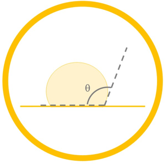
Enhancing Water-Contact Angles for 193i
193 immersion lithography (193i) involves replacing the air gap between the final lens element of a lithographic laser and the photoresist layer with water (refractive index ~ 1.44). To minimize the physical and chemical interactions occurring between water and the photoresist, or the absorption of water into the resist, chip manufacturers use a hydrophobic photoresist topcoat or incorporate a hydrophobic monomer into the photoresist coating itself. Halocarbon manufactures novel high-quality, high-purity HFIP-based monomer systems that can provide very high water contact angles (a measure of hydrophobicity). By increasing the water contact angles (both advancing and receding), lithographic steps can be carried out by eliminating water absorption and allow for higher scanning speeds, reducing defects, and improving production throughput. Halocarbon materials, when incorporated into photoresists and top coats, have been demonstrated to provide superior hydrophobicity and exceptional patterning control.

Compatible with Historic Development Solvents
The History of Development Solvents and The Drop-In of HFIP-based Materials
The HFIP-based monomers and monomer precursors developed and manufactured by Halocarbon allow for control over hydrophobicity and hydrophilicity. A key part of the photolithography process is the clean removal of the photoresist layer from the surface of a patterned wafer. This stage of the process, known in the industry as the development step, involves the dissolution of the patterned portions of the photoresist using aqueous base (most commonly tetramethylammonium hydroxide, or TMAH). The acidity of the alcohol group in HFIP-based materials can be used to modulate the overall solubility of the photoresist layer at different pHs of aqueous alkalinity. This pH-triggered solubility switching allows a photoresist layer to function as a hydrophobic coating within an acidic to neutral pH-range, and as a hydrophilic and aqueous-soluble material at the alkaline pH-range, ensuring high-fidelity across both the patterning and development stages of the photolithography process.